
Modern electronic systems rely on tightly regulated supply rails and clean signal lines to maintain operational stability. However, transient electrical overstress poses an ongoing threat to silicon integrity, sensitive microcontrollers, and communication interfaces. Transient spikes can originate from electrostatic discharge (ESD), inductive load switching, lightning coupling, or abrupt power grid fluctuations. Even a nanosecond transient exceeding maximum voltage ratings can punch through delicate gate oxides and cause irreversible junction failure. Transient Voltage Suppression (TVS) diodes provide the primary hardware defense against these destructive surge events.
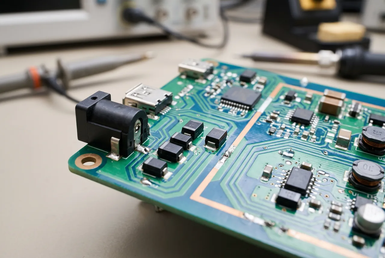
Technical Parameter Comparison: TVS Diode Selection Guide
Selecting the proper TVS diode requires balancing circuit operating tolerances against transient energy absorption limits:
| Electrical Parameter | Symbol | Definition & Function | Circuit Design Rule |
| Reverse Working Voltage | $V_{\text{RWM}}$ | Maximum continuous DC or peak AC voltage where the diode remains non-conductive | Must be equal to or slightly higher than the nominal operating voltage of the protected line |
| Breakdown Voltage | $V_{\text{BR}}$ | Voltage threshold at which the diode enters avalanche conduction and shunts current | Measured at test current $I_T$; must stay above maximum normal rail ripple |
| Clamping Voltage | $V_{\text{C}}$ | Maximum voltage across the TVS diode while shunting peak surge current ($I_{\text{PP}}$) | Must never exceed the absolute maximum breakdown rating of downstream ICs |
| Peak Pulse Power | $P_{\text{PP}}$ | Total surge dissipation capacity for a standardized pulse waveform (e.g., $10/1000\,\mu\text{s}$) | Must exceed the expected transient surge energy of the operating environment |
| Parasitic Capacitance | $C_{\text{J}}$ | Internal junction capacitance between diode terminals | Must remain ultra-low ($<1\,\text{pF}$) on high-speed data lines (USB 3.0, HDMI, Ethernet) |
Operating Principle: How TVS Diodes Clamp Surges
A TVS diode operates via solid-state P-N junction avalanche breakdown. Unlike standard rectifiers or Zener diodes designed for continuous power dissipation or steady voltage regulation, TVS devices are optimized to divert high-energy transients within picoseconds:
-
High-Impedance State (Normal Operation): During routine operation, the circuit voltage remains below the reverse working voltage ($V_{\text{RWM}}$). The TVS diode exhibits high internal impedance, drawing only microamperes of leakage current and remaining functionally invisible to the system.
-
Low-Impedance Avalanche Shunt (Transient Event): When a fast transient (such as an ESD event) exceeds the breakdown voltage ($V_{\text{BR}}$), the P-N junction enters an avalanche state. Its dynamic resistance drops to near zero, shunting peak transient current directly to ground and clamping the voltage across the load to a safe level ($V_{\text{C}}$).
-
Automatic Reset: Once the surge dissipates and circuit voltage falls back below $V_{\text{BR}}$, the TVS diode recovers to its high-impedance state without requiring a power cycle or fuse replacement.
Common Sources of Transient Overstress
Circuit designers must account for three primary transient sources across consumer, industrial, and automotive environments:
1. Electrostatic Discharge (ESD)
Human contact with exposed connectors, I/O ports, or control panels releases fast static charges. Standardized under IEC 61000-4-2, an ESD strike features rise times under one nanosecond and peak amplitudes reaching 8 to 15 kV. TVS diodes placed across exposed data and power pins absorb this initial strike before it enters the system board.
2. Inductive Switching Transients
Switching off inductive components—such as relays, solenoids, DC motors, or transformers—causes the magnetic field to collapse rapidly. This generates a severe back-EMF voltage spike ($V = -L \frac{di}{dt}$). Without a local TVS diode to suppress this inductive kick, nearby driver transistors, MOSFETs, and power supplies face rapid breakdown.
3. Power Distribution Surges and Lightning Coupling
Indirect lightning strikes and high-power industrial grid switching induce long-duration surges onto building wiring and outdoor cabling (governed by IEC 61000-4-5 waveforms like $8/20\,\mu\text{s}$ and $10/1000\,\mu\text{s}$). While secondary to building-level surge arresters, board-level TVS diodes absorb the residual transient energy that reaches the PCB.
Unidirectional vs. Bidirectional TVS Diodes
Choosing between unidirectional and bidirectional topologies depends entirely on signal polarity:
Unidirectional (DC Rails)           Bidirectional (AC & Differential Data)
         Cathode (Band)
           ├──[|<]──                         ──[>|][|<]──
           │       │
          (+)     (-)
-
Unidirectional Diodes: Feature an asymmetric V-I characteristic with a distinct cathode band. In the reverse direction, they clamp high-voltage transients; in the forward direction, they behave like a standard diode with a $0.7\,\text{V}$ forward drop. They are ideal for single-polarity DC power supplies and unidirectional digital logic.
-
Bidirectional Diodes: Consist of two back-to-back P-N junctions configured in series, presenting symmetrical avalanche breakdown in both positive and negative directions. They are mandatory for AC signal paths, audio lines, and differential communications (RS-485, CAN bus) where voltages alternate above and below ground reference.
Printed Circuit Board (PCB) Layout Rules for Transient Suppression
Even the most robust TVS diode will fail to protect sensitive electronics if PCB layout practices introduce parasitic inductance. Engineers should follow these structural routing guidelines:
-
Place Diodes Immediately at the Connector: Mount the TVS diode as physically close to the external input connector or cable entry point as possible. Divert transient energy at the board boundary before it couples into neighboring copper traces.
-
Minimize Lead and Trace Inductance: High-frequency transients perceive trace length as inductance ($V_{\text{spike}} = L_{\text{trace}} \frac{di}{dt}$). Keep traces between the signal line, the diode pad, and the reference ground plane wide, straight, and as short as possible.
-
Dedicated Ground Returns: Route the diode’s ground connection directly to a low-impedance chassis or system ground plane using multiple parallel vias. Avoid running surge ground currents through sensitive analog ground tracks.
-
Capacitance Constraints on High-Speed Interfaces: On high-speed serial buses (USB, PCIe, Ethernet), high parasitic diode capacitance causes signal degradation, rise-time degradation, and impedance mismatches. Use specialized low-capacitance TVS diode arrays ($C_{\text{J}} < 0.3\,\text{pF}$) specifically engineered for high-bandwidth differential pairs.
Selecting a TVS diode with the proper working voltage, low clamping threshold, and appropriate package footprint forms the foundation of reliable hardware design. By pairing rigorous parameter calculations with tight board-level routing discipline, engineering teams safeguard critical microelectronics against real-world transient stress and ensure long-term device longevity.