
As artificial intelligence (AI) workloads expand and data centers consume increasing amounts of electricity, semiconductor designers are under growing pressure to improve processor performance without proportionally increasing power consumption. The industry is therefore focusing not only on raw computing speed but also on energy efficiency, measured through metrics such as performance per watt, energy per task, and—particularly for AI accelerators—tera operations per second per watt (TOPS/W).
Designing next-generation central processing units (CPUs), graphics processing units (GPUs), and neural processing units (NPUs) requires improvements across the entire computing system. Transistor architecture, power delivery, chip packaging, memory bandwidth, and specialized processing units all influence how efficiently a processor performs its work.
For decades, semiconductor manufacturers benefited from Dennard scaling, a principle under which transistor dimensions and operating voltages could shrink together while maintaining approximately constant power density. This helped improve performance without a proportional increase in power consumption. As voltage scaling became more difficult and transistor dimensions continued to shrink, those gains became harder to sustain.
Modern processors can no longer depend on transistor miniaturization alone to deliver substantial efficiency improvements. Instead, designers are combining advances in transistor structures, advanced packaging, backside power delivery, high-bandwidth memory, and workload-specific computing architectures.
The Evolution of Processor Efficiency
Processor design has evolved through several overlapping technological eras. Each has introduced new ways to improve performance, reduce energy consumption, and address the physical limits of semiconductor manufacturing.
| Technology trend | Key development | Primary benefit | Important challenge |
|---|---|---|---|
| Planar CMOS | Traditional planar MOSFET transistors | Improved integration and clock-speed scaling | Leakage, power consumption, and heat |
| FinFET | Three-dimensional fin-shaped transistor channels | Better electrostatic control and continued scaling | Manufacturing complexity and power-management limits |
| Gate-All-Around (GAA) | Nanosheet or nanoribbon channels surrounded by the gate | Improved channel control and potential efficiency gains | Process complexity and interconnect resistance |
| Chiplets and advanced packaging | Multiple dies integrated within one package | Flexible integration and improved manufacturing economics | Packaging cost, communication overhead, and thermal management |
| Heterogeneous computing | CPUs, GPUs, NPUs, and other specialized engines | Better energy efficiency for targeted workloads | Software optimization and workload scheduling |
These technologies are complementary rather than strictly sequential. A modern processor can combine advanced transistors, multiple chiplets, stacked memory, and specialized accelerators within a single package.
Gate-All-Around Transistors: Improving Channel Control
One major development in advanced semiconductor manufacturing is the transition from FinFETs to Gate-All-Around (GAA) transistor architectures.
In a FinFET, the gate surrounds three sides of a raised semiconductor channel. In a GAA design, the gate surrounds the channel on all sides. Common implementations use stacked nanosheets or nanoribbons.
This structure improves the gate’s control over the channel, which can help reduce leakage and support continued transistor scaling.
Better electrostatic control
As transistor dimensions shrink, controlling current flow becomes increasingly difficult. GAA structures provide stronger electrostatic control than conventional FinFETs in many implementations, helping designers manage short-channel effects and reduce unwanted current when a transistor is off.
However, GAA transistors do not eliminate leakage or quantum tunneling. Their effectiveness depends on channel dimensions, materials, operating voltage, and the specific manufacturing process.
Adjustable channel dimensions
Nanosheet transistors can offer flexibility in channel width. By adjusting the width and configuration of the sheets, designers can balance drive current, capacitance, density, and power consumption for different circuit requirements.
This flexibility helps manufacturers optimize logic cells for different workloads, although the achievable benefits depend on the process technology and design rules.
Operating voltage and dynamic power
Reducing supply voltage can significantly lower dynamic power consumption. A simplified relationship is:
[
P_{\text{dynamic}} \approx \alpha C V_{\text{dd}}^2 f
]
Here, (\alpha) represents switching activity, (C) is effective capacitance, (V_{\text{dd}}) is supply voltage, and (f) is switching frequency.
Because voltage appears squared in this relationship, lowering it can reduce dynamic power substantially. However, reducing voltage too far can compromise performance or reliable operation. Designers must also account for leakage, timing requirements, and the voltage needed to keep a particular circuit stable.
GAA technology can help improve this balance, but the overall efficiency gain depends on the complete chip design.
Backside Power Delivery: Reducing Routing Congestion
Traditional processors route both power-distribution networks and signal interconnects through the front-side metal layers above the transistor structures. As designs become denser, these networks compete for limited routing space.
Backside power delivery addresses this challenge by moving significant portions of the power-distribution network to the rear of the silicon die.
A simplified comparison illustrates the concept:
Traditional power delivery
[Front-side power and signal routing]
                 ↓
          [Transistor layer]
                 ↓
           [Silicon substrate]


Backside power delivery
[Front-side signal routing]
                 ↓
          [Transistor layer]
                 ↓
       [Power connections to backside]
                 ↓
      [Backside power-distribution grid]
The exact structure varies by manufacturer and process technology.
Reducing voltage drop
Electrical resistance in power-delivery networks can cause voltage drops between the power source and the active transistors. These drops, commonly called IR drop, can reduce the voltage available to circuits and complicate reliable high-performance operation.
A carefully designed backside power network can reduce power-delivery resistance and improve the distribution of voltage across a chip.
Freeing front-side routing resources
Moving power distribution to the backside also frees front-side routing resources for signals. This can reduce congestion and help improve layout efficiency, with potential benefits for performance, density, and power consumption.
The benefits are not automatic. Backside power delivery introduces additional manufacturing and integration challenges, and the results depend on the specific implementation.
As advanced processors become increasingly dense, this technology is becoming an important part of semiconductor scaling strategies.
Chiplets: Building Processors from Multiple Dies
Manufacturing a large processor as one monolithic die can become expensive and difficult as transistor counts and die dimensions increase. Larger dies generally expose more area to potential manufacturing defects, which can affect yield and cost.
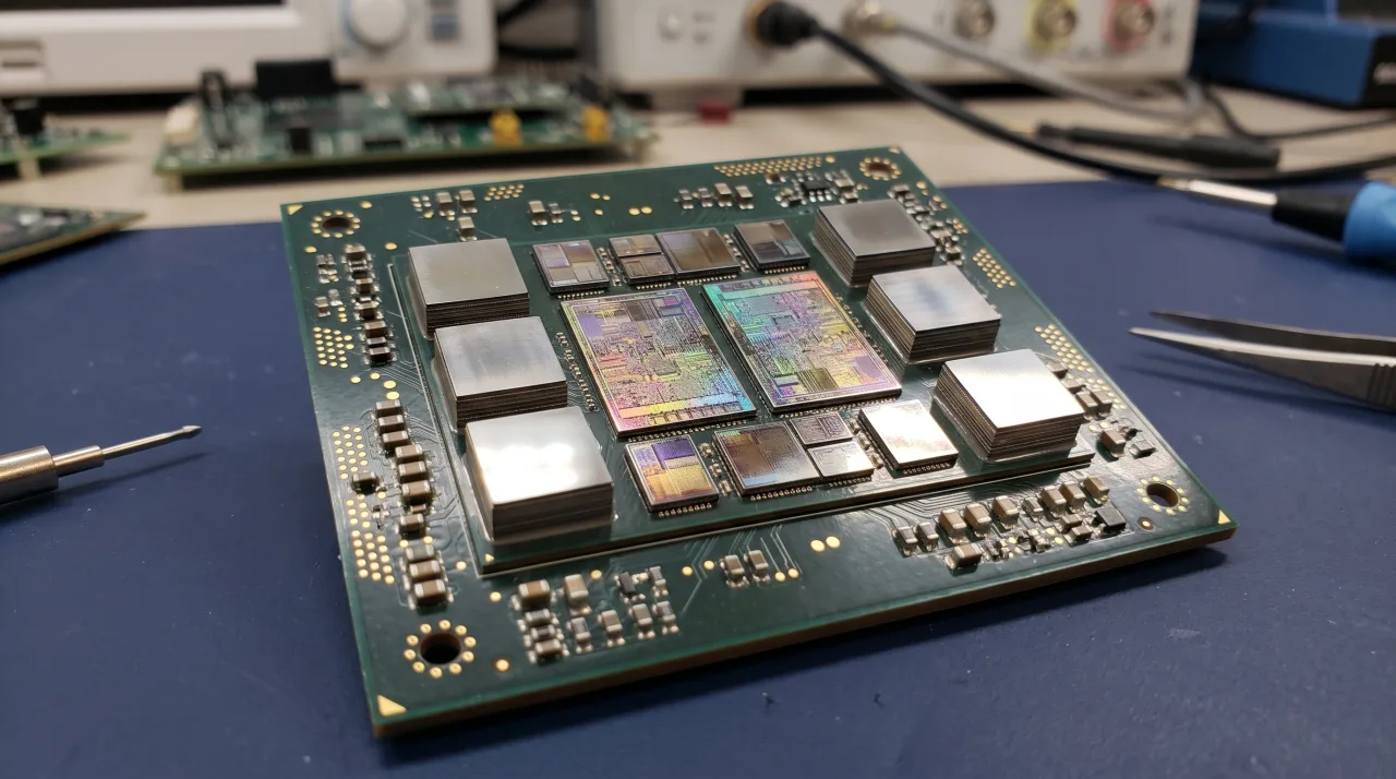
Chiplet architectures address this challenge by dividing a processor into smaller dies that are connected within a package.
Different chiplets can perform different functions, including computation, cache storage, memory control, and input/output operations.
Matching functions to manufacturing processes
Not every processor component benefits equally from the most advanced manufacturing process.
Compute-intensive logic may benefit significantly from leading-edge transistors, while analog circuits, input/output interfaces, and some memory-related functions may be better suited to other process technologies.
Chiplets allow designers to manufacture these components using different processes and integrate them into one system. This can improve design flexibility and manufacturing economics, although packaging, testing, and integration costs must also be considered.
Advanced packaging and die-to-die communication
Technologies such as TSMC’s Chip on Wafer on Substrate (CoWoS) and Intel’s Embedded Multi-die Interconnect Bridge (EMIB) support high-density connections between dies. Three-dimensional integration and hybrid bonding provide additional options for reducing connection distances and increasing interconnect density.
The Universal Chiplet Interconnect Express (UCIe) standard defines an approach to die-to-die connectivity intended to support interoperability across a broader chiplet ecosystem.
Interconnect performance depends on factors such as link width, data rate, package construction, signaling method, and operating conditions. Energy per bit therefore varies by implementation; no single efficiency figure applies to all chiplet connections.
Chiplets are particularly valuable for processors that need to combine large amounts of compute logic, cache, and high-bandwidth memory within a compact package.
High-Bandwidth Memory: Addressing the Memory Wall
Processor performance depends on more than the speed of its arithmetic units. The processor must also receive data quickly enough to keep those units busy.
In many AI and high-performance computing workloads, moving data between memory and compute units consumes substantial time and energy. This challenge is commonly known as the memory wall.
High-bandwidth memory (HBM) helps address this problem by stacking multiple dynamic random-access memory (DRAM) dies vertically and connecting them through thousands of through-silicon vias (TSVs) and other package interconnects.
HBM is typically integrated into the same package as a processor, often using an interposer or another advanced packaging structure. It is generally positioned alongside the compute die rather than directly stacked on top of it.
Wide interfaces and high bandwidth
Unlike conventional memory interfaces that rely on comparatively narrow data paths, HBM uses a very wide interface to transfer large quantities of data in parallel.
For example, Micron specifies HBM3E solutions with a 1,024-bit interface and bandwidth exceeding 1.2 terabytes per second per memory stack. Actual bandwidth depends on the product and its operating specifications.
This architecture can deliver high memory bandwidth while reducing the need for long, high-speed connections across a conventional circuit board.
Improving energy efficiency
Placing memory close to the processor reduces the physical distance data must travel and can lower the energy required for each transferred bit compared with some conventional memory configurations.
HBM does not eliminate memory bottlenecks. Performance still depends on memory capacity, access patterns, controller design, caching, and the ability of software to use available bandwidth effectively.
As AI models grow and process larger datasets, the balance between compute performance, memory capacity, bandwidth, and power consumption is becoming increasingly important.
Workload-Specific Acceleration: Matching Hardware to the Task
General-purpose CPUs are designed to execute a broad range of instructions and manage diverse workloads. GPUs excel at highly parallel operations, while NPUs and other specialized accelerators are designed to perform particular AI computations efficiently.
Matching workloads to the right hardware can improve both performance and energy efficiency.
1. Matrix and tensor acceleration
Many AI workloads rely heavily on matrix multiplication and tensor operations. GPUs and NPUs incorporate specialized execution units designed to perform these operations in parallel.
By processing many calculations simultaneously, these units can achieve greater throughput per watt than a general-purpose processor executing the same workload through conventional instruction pipelines.
The actual advantage depends on the hardware architecture, the model, data precision, memory behavior, and software implementation.
2. Dynamic voltage and frequency scaling
Dynamic voltage and frequency scaling (DVFS) adjusts a processor’s operating voltage and clock frequency according to workload demand and operating conditions.
When a workload requires high performance, the processor may increase frequency and voltage within its operating limits. During lighter workloads, it can reduce them to save energy.
Power-management systems may also use clock gating, power gating, and other techniques to reduce consumption in inactive or underutilized circuit blocks.
These mechanisms help processors balance responsiveness, power consumption, and thermal limits.
3. Lower-precision arithmetic
AI applications do not always require the same numerical precision used in traditional scientific computing.
Depending on the model and task, lower-precision formats such as FP8 floating-point or INT4 integer arithmetic can reduce memory requirements and increase processing throughput. They can also improve energy efficiency when supported by suitable hardware.
However, lower precision can affect numerical accuracy and model quality. Quantization methods, calibration, model architecture, and workload characteristics determine whether the resulting trade-off is acceptable.
Consequently, efficiency improvements should be measured using representative workloads rather than assuming a fixed percentage of energy savings across all applications.
The Growing Importance of System-Level Optimization
The race to build more efficient processors is no longer defined by transistor counts or clock frequency alone. Efficiency increasingly depends on how well the entire computing system is designed.
GAA transistors can improve channel control. Backside power delivery can ease routing congestion and improve voltage distribution. Chiplets provide flexibility in manufacturing and system integration, while HBM increases the amount of data that can reach compute units. Specialized accelerators allow workloads to execute using hardware suited to their computational needs.
These technologies also introduce trade-offs. Advanced packaging can increase manufacturing complexity, dense compute systems require careful thermal management, and specialized accelerators depend on effective software support. Improvements at the transistor level do not necessarily translate into equivalent gains at the system level.
For AI data centers, mobile devices, and high-performance computing platforms, the most useful measure of progress is therefore not simply how many operations a processor can perform, but how efficiently it completes the tasks users and organizations actually need.
As semiconductor designers combine advances in transistor architecture, power delivery, packaging, memory, and workload-specific processing, they are creating new ways to deliver more computing capability within increasingly demanding power and thermal limits.